MAXVY DDR5CKD01 Clock Driver

Description

MAXVY DDR5CKD01 is a registering clock driver used on DDR5 CUDIMMs, CSODIMMs, and CAMM. Its primary function is to buffer the DDR clock between the Host controller and the DRAMs.

Features

  • Compliance as per JEDEC’s JESD82-531B - Version 1.21
  • CKD PLL modes
    • PLL ByPass Mode
    • Single PLL Mode
    • Dual PLL Mode
  • Clock Stop Operation.
  • PLL Modes output frequency range 1000 MHz to 4600 MHz supported.
  • PLL Modes Frequency change supported.
  • LID’s determination based on ZQCAL RL value.
  • Sideband Interface I3C mode up to 12.5 MHz and I2C mode up to 1 MHz speed supported
  • Parity Check is enabled
  • Packet Error Check is supported (PEC)
  • Supported Switch from I2C to I3C Basic Mode and vice versa
  • Support CKD write and read operations with or without PEC enabled
  • In-band Interrupt (IBI)
  • Interrupt Arbitration
  • I3C Basic Common Command Codes (CCC)
    • ENEC
    • DISEC
    • RSTDAA
    • SETAASA
    • GETSTATUS
    • DEVCAP
    • SETHID
    • DEVCTRL
  • Bus Reset, Bus clear supported
  • Clearing Status Register
  • Packet Error Check & Parity Error Handling
  • CCC Packet Error Handling

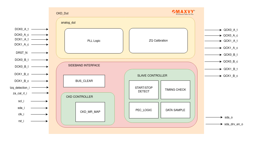
Block Diagram

CKD Block Diagram

Application

  • DDR5 CUDIMM
  • CSODIMM
  • CAMM

Resource Deliverables

  • Verilog Source code
  • User Guide
  • IP Integration Guide
  • Simulation Script
  • Synthesis Script
  • Encrypted UVM Verification Environment
  • cocotb Verification Environment
  • Basic Testsuite
  • Firmware code